Problem 3.4 in the textbook. (Reproduced below for your convenience.)
When KOH etching is used on 500 um thick (100) oriented silicon wafer,
- what mask feature size is required to produce a 400 um squarediaphragm of thickness 20 um?
- what is the edge-length variation for the diaphragm if the actual wafer thicknness for different wafers varies between 490 and 510 um?
- assuming that the sensitivity of a pressure sensor varies as the inverse fourth power of the diaphragm edge-length, what percentage variation in sensitivity can be attributed to variations in wafer thickness?
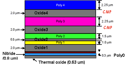
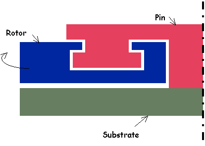
Sandia lab's SUMMiT V process helps make very sophisticated micromechanisms consisting of gears and linkages. Central to this process is a nice in-plane revolute (pin) joint that has very little play (clearance) in radial as well as axial directions. The layer thicknesses in this process and the approximate desired cross-section of the revolute joint are shown below. Draw the masks and process flow with cross-section. Note that SUMMiT V uses two planarization steps, which are indicated with CMP in the figure below.

